Alexandre Dmitriev on Hole-Mask Colloidal Lithography
Emerging Research Fronts Commentary, August 2011

|
Article: Hole-mask colloidal lithography
Authors: Fredriksson, H;Alaverdyan, Y;Dmitriev,
A;Langhammer, C;Sutherland, DS;Zaech, M;Kasemo,
B Photo by Jan-Olof Yxell. |
Alexandre Dmitriev talks with ScienceWatch.com and answers a few questions about this month's Emerging Research Front paper in the field of Materials Science.
![]() Why do you think your paper is highly
cited?
Why do you think your paper is highly
cited?
It is essentially a "method paper"—it describes a recipe for bottom-up nanofabrication of low-dimensional structures at surfaces in ambient conditions. The key is that this recipe is simple enough, affordable, and can bring benefits in a plethora of research and technology areas, where one needs objects of 20-5000 nm, fabricated on an arbitrary surface and covering cm2 area.
To date by far the largest application field for hole-mask colloidal lithography is nanoplasmonics—the science of light coupling to matter with the help of surface plasmons, collective oscillations of electrons at the interface of metal and dielectric. This area is really dynamic and has been growing fast for the past 10 years. This nanofabrication technique already has been applied in nano-optics, biological and chemical sensing, catalysis, design of optical metamaterials, magnetoplasmonics, plasmon-enhanced photovoltaics and photochemistry, and even spintronics.
![]() Does it describe a new discovery, methodology, or
synthesis of knowledge?
Does it describe a new discovery, methodology, or
synthesis of knowledge?
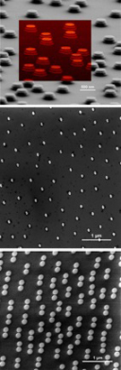
Hole-mask colloidal lithography is able to produce
arrays of optical Yagi-Uda nanoantennas (top, image courtesy of L. Tong,
Chalmers University of Technology, Göteborg, Sweden), nickel
nanoellipses and nanodisks pairs (middle and bottom, image courtesy of H.
Fredriksson, Eindhoven Technical University, Eindhoven,
Netherlands).
The paper describes a methodology—truly versatile self-assembly-based nanofabrication technique that is tolerant to the choice of materials one uses for the nanostructures (metals, semiconductors, dielectrics) and to the choice of supporting surfaces (rigid—glass, Si, metal; or flexible—for example, various polymer layers). The fact that the method uses standard processes like polymers spin-coating or self-assembly of colloidal nanospheres from aqueous solutions allows one to integrate it seamlessly with other production steps in, for example, photovoltaics, or other nanofabrication methods like e-beam of photolithography.
![]() Would you summarize the significance of your paper
in layman's terms?
Would you summarize the significance of your paper
in layman's terms?
The paper provides researchers in various fields of nanoscience with the method to produce arrays of extremely small (nanoscopic) objects that cover large areas (up to several cm2). These objects are typically dispersed on the surface in disordered fashion, yet keeping a certain characteristic distance between them. These objects can be disks, ellipses, pairs of structures, cones, and others.
The ability to fabricate such small features that cover such large areas and yet to do it cheaply and fast opens broad application possibilities. Examples of these include: plasmon-enhanced solar cells of various types, (photo)catalysis, or advanced platforms for information storage and processing.
![]() How did you become involved in this research, and
how would you describe the particular challenges, setbacks, and
successes that you've encountered along the way?
How did you become involved in this research, and
how would you describe the particular challenges, setbacks, and
successes that you've encountered along the way?
I joined Chalmers research team as a Marie Curie Fellow in mid-2004. Colloidal lithography techniques had been under development there for the previous 3-4 years, and the method known today as hole-mask colloidal lithography was originally designed by Hans Fredriksson at that time. With this as a starting point a concerted team effort made it possible to diversify the library of nanostructures geometries that were possible to produce with the method. The simplicity of the technique and its applicability in various research fields sealed its reputation among researchers at Chalmers.
The challenge was however to convince research groups outside Chalmers to test the method—during the past five years we've done this by helping researchers from the universities around Europe and beyond to grasp the fine details of hole-mask colloidal lithography. I'm proud to state that the method has established itself as a nanofab workhorse in nanoplasmonics.
![]() Where do you see your research leading in the
future?
Where do you see your research leading in the
future?
Bottom-up nanofabrication certainly provides great opportunities for future technologies. Affordable and largely parallel self-assembly-based methods are well-positioned to become the key manufacturing technologies in such diverse areas as sustainable energy production and storage, biomedical nanotechnology or information technologies. As far as hole-mask colloidal lithography is concerned, new available nanoarchitectures will boost new applications—as shown on the Figure, optical Yagi-Uda nanoantennas, plasmonic nanoferromagnets, and others.
In particular, compatibility with other industry-standard fabrication and processing methods and the possibility for scaling-up of the hole-mask colloidal lithography are the questions we address in our projects that target photovoltaics and biological/chemical sensing.
![]() Do you foresee any social or political
implications for your research?
Do you foresee any social or political
implications for your research?
As mentioned above, the nanofabrication method we developed has good
prospects to contribute to the creation of more efficient solar cells or to
be the basis for the future point-of-care medical diagnostics/sensing
devices. Both areas obviously have tremendous social and economical
impact—and we as researchers are proud to be the part of such
development.![]()
Alexandre Dmitriev
Assistant professor
Department of Applied Physics
Chalmers University of Technology
Göteborg, Sweden
Web
KEYWORDS: HOLE-MASK COLLOIDAL LITHOGRAPHY, BOTTOM-UP NANOFABRICATION, ENHANCED RAMEN SCATTERING, NANOSPHERE LITHOGRAPHY, SILVER NANOPARTICLES, OPTICAL PROPERTIES, GOLD NANOPARTICLES, NANOMETRIC HOLES, GOLD NANORODS, FABRICATION, ARRAYS, SEMICONDUCTOR.