Yu-Ming Lin on High-Performance Graphene Transistors
Emerging Research Fronts Commentary, December 2011


|
Article: 100-GHz Transistors from Wafer-Scale Epitaxial Graphene
Authors: Lin, YM;Dimitrakopoulos,
C;Jenkins, KA;Farmer, DB;Chiu, HY;Grill, A;Avouris, P |
Yu-Ming Lin talks with ScienceWatch.com and answers a few questions about this month's Emerging Research Front paper in the field of Physics.
![]() Why do you think your paper is highly
cited?
Why do you think your paper is highly
cited?
This paper is well-cited because it presents the first demonstration of high-performance graphene transistors, up to a cut-off frequency of 100 GHz, fabricated on wafer-scale graphene. Graphene is a single layer of carbon atoms arranged like a honeycomb, and has generated enormous research activities and gathered strong interests from the industry in the last few years, mainly because of its unique electrical and mechanical properties.
The 2010 Nobel Prize in Physics was awarded to Andre Geim and Konstantin Novoselov for the isolation and characterization of graphene, and our paper was cited as the example of future graphene applications in the announcement. This work is therefore of significance to the development of graphene technology and of great interest to the audience in the graphene research community.
![]() Does it describe a new discovery, methodology, or
synthesis of knowledge?
Does it describe a new discovery, methodology, or
synthesis of knowledge?
In this paper, we demonstrated a radio-frequency graphene transistor with the highest cut-off frequency achieved at the time—100 billion cycles per second—for any graphene devices. The cut-off frequency signifies the maximum frequency that a transistor could operate to transmit electrical signals. Most importantly, this high-frequency record was achieved using wafer-scale, epitaxially grown graphene with processing technology compatible to that used in advanced silicon device fabrication.
The graphene transistor utilized a metal top-gate architecture and a novel gate insulator stack involving a polymer and a high dielectric constant oxide. The gate length was modest, 240 nanometers, leaving plenty of space for further optimization of its performance by scaling down the gate length. It is noteworthy that the frequency performance of the graphene device already exceeds the cut-off frequency of state-of-the-art silicon transistors of the same gate length (~ 40 billion cycles per second).
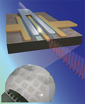
The upper image of the figure represents the schematic
of a graphene field-effect transistor, which can be used to amplify
electrical signals with very high frequencies (up to 100 GHz). The lower
image shows arrays of graphene devices, including the RF transistors,
fabricated on a two-inch graphene wafer.
In our recent work published in Nature (472: 74, 2011), we further reduced the gate length down to 40 nanometers, the smallest transistor ever fabricated, and achieved a cut-off frequency above 150 GHz. Earlier this year, we also demonstrated the first graphene integrated circuit fabricated on a single SiC wafer (Science 332: 1294, 2011) operating as a frequency mixer at 10 GHz.
![]() Would you summarize the significance of your paper
in layman’s terms?
Would you summarize the significance of your paper
in layman’s terms?
Graphene possesses unusual electronic properties that may eventually lead to vastly faster transistors than those achieved so far. In spite of the high potential and strong interest in graphene, it remains unclear if graphene devices can be manufactured on the wafer scale and in large quantities, which is critical for commercialization of any technology.
This work provides convincing demonstration that wafer-scale, high-performance graphene transistors can be produced using processes compatible with techniques developed for the semiconductor industries. This clearly shows that graphene can be utilized to produce high-performance devices and integrated circuits using technologically relevant methodologies and conditions.
![]() How did you become involved in this research, and
were there any problems along the way?
How did you become involved in this research, and
were there any problems along the way?
Since 2005, I was already exploring electrical transport properties of graphene and its nano-ribbons. I became involved with the development of graphene RF technology when IBM was funded by DARPA to pursue Carbon-based Electronics for Radio-frequency Applications (CERA) in May 2008. In the same year, we achieved the first milestone by demonstrated graphene transistor operating in the GHz frequencies, and this accomplishment was previously highlighted by ScienceWatch.com in as the 2010 May New Hot Paper in Chemistry.
One major challenge of this work is the synthesis of high-quality graphene films on SiC wafers. My colleagues Christos Dimitrakopoulos and Alfred Grill have made great progress in optimizing synthesis conditions to produce graphene wafers appropriate for electronic devices.
Another challenge involved the development of device fabrication processes without inducing degradation to graphene, which acted as the transistor channel for carrier transport. In this respect, my co-worker Damon Farmer devised a novel process that allows for the deposition of high-quality oxide on graphene by combining an organic buffer layer and the atomic layer oxide deposition (ALD) technique, which preserved the desirable properties of graphene in the final device.
With help from Keith Jenkins and Alberto Valdes-Garcia, we designed the transistor layout and performed the RF characterization. The work also benefited greatly from the insightful discussions and guidance of Phaedon Avouris and Chun-Yung Sung.
![]() Where do you see your research leading in the
future?
Where do you see your research leading in the
future?
Graphene holds great potential for future electronics, and we have witnessed giant leaps in graphene technology in the last couple of years. For example, large-area graphene is readily accessible by more than one synthesis methods, including epitaxial growth on SiC and chemical vapor deposition (CVD) on metal surfaces. The performance of graphene transistors has also been advancing at an unprecedented pace, from a few GHz to hundreds of GHz within only two years.
I hope the impact of this research could encourage more efforts and interests in developing graphene-related technology, and finally lead to commercialization of graphene-based products in the next few years in areas like communication and, perhaps, digital computing applications.
![]() Do you foresee any social or political
implications for your research?
Do you foresee any social or political
implications for your research?
While I do not expect to see any immediate social or political impact from
our research, I hope that this research may open up new directions for
electronic industry beyond the conventional semiconductor materials such as
Si, and potentially generate niche applications based on high-performance
graphene devices.![]()
Yu-Ming Lin
Research Staff Member
IBM T. J. Watson Research Center
Yorktown Heights, NY, USA
KEYWORDS: GRAPHENE, TRANSISTORS, APPLICATIONS, HIGH FREQUENCY RECORD, WAFER-SCALE EPITAXIAL GRAPHENE, METAL TOP-GATE ARCHITECHTURE, GATE INSULATOR STACK, POLYMER, HIGH DIELECTRIC CONSTANT OXIDE.