Minjoo Larry Lee on Extraordinary Mobilities in Strained SiGe Heterostructures
Fast Moving Front Commentary, July 2010

|
Article: Strained Si, SiGe, and Ge channels for high-mobility metal-oxide-semiconductor field-effect transistors
Authors: Lee, ML;Fitzgerald, EA;Bulsara,
MT;Currie, MT;Lochtefeld, A |
Minjoo Larry Lee talks with ScienceWatch.com and answers a few questions about this month's Fast Moving Fronts paper in the field of Physics.
![]() Why do you think your paper is highly
cited?
Why do you think your paper is highly
cited?
I think that the paper is highly cited because the work resides in an area of great importance to both industry and academia. At the time, the use of strain to enhance carrier mobility in microprocessor technology was growing in importance worldwide.
Our paper focused on the connections between strain, layer structure, and transistor mobility characteristics. These issues are relevant to researchers in fields ranging from materials growth and characterization to device physics and processing.
![]() Does it describe a new discovery, methodology, or
synthesis of knowledge?
Does it describe a new discovery, methodology, or
synthesis of knowledge?
The paper integrated knowledge gained from fundamental studies of strained heterostructure growth, carrier transport, and device physics. We sought to understand how the extraordinary mobilities that had previously been measured in strained SiGe heterostructures could impact complementary metal-oxide-semiconductor (CMOS) technology.
Ultimately, this paper synthesized years of research, culminating in a map of the possible mobility enhancements that are available in strained Si, SiGe, and Ge.
![]() Would you summarize the significance of your paper in
layman’s terms?
Would you summarize the significance of your paper in
layman’s terms?
The processors in many of our computers and other electronic gadgets have benefited from the use of strain technology. This paper took the discoveries made by myself and many other researchers worldwide to paint a picture of what the ultimate limits of strain technology will be for future generations.
![]() How did you become involved in this research, and how
would you describe the particular challenges, setbacks, and successes
that you've encountered along the way?
How did you become involved in this research, and how
would you describe the particular challenges, setbacks, and successes
that you've encountered along the way?
I became involved with this research when I joined the laboratory of Gene Fitzgerald at MIT as a graduate student in materials science and engineering. A particular challenge in this work for me was the need to think and work in an interdisciplinary manner.
Fortunately, overcoming some of these challenges created very exciting research opportunities for me. Along the way, I benefited greatly from interactions with the faculty at MIT as well as with numerous scientists working in industry.
![]() Where do you see your research leading in the
future?
Where do you see your research leading in the
future?
The CMOS industry is looking beyond Si for future performance increases at materials including III-Vs, Ge, and graphene. The compressively strained Ge field-effect transistors reviewed in this paper still stand among the contenders for the future of CMOS technology, due to their very high hole mobilities.
On the basic research side, one intriguing future direction is in the
growth, properties, and device applications of Ge under biaxial tension. In
order to attain high tensile strain, such layers have to be grown on III-V
templates, creating a wide range of new challenges and opportunities for
fundamental research.![]()
Minjoo Larry Lee
Assistant Professor of Electrical Engineering
Yale University
New Haven, CT, USA
KEYWORDS: STRAINED, SI, SIGE, GE, METAL-OXIDE SEMICONDUCTOR FIELD-EFFECT TRANSISTORS, MOSFETS, HIGH ELECTRON MOBILITY, MOLECULAR BEAM EPITAXY, THREADING DISLOCATION DENSITIES, SILICON INVERSION LAYERS, MODULATION DOPED SI/SIGE, ON INSULATOR LAYERS, HIGH HOLE MOBILITY, P-TYPE, RELAXED SI1-XGEX, N-MOSFETS.
Figure 1:
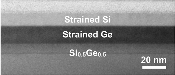
Figure 1: Cross-sectional transmission electron microscopy image of a very high-mobility strained Si/strained Ge dual-channel heterostructure grown on relaxed Si0.5Ge0.5.
Reprinted with permission from "Strained Si, SiGe, and Ge channels for high-mobility metal-oxide semiconductor field-effect transistors" (J. Appl. Phys. 97[1]: art. no. 011101, 1 January 2005). Copyright 2010, American Institute of Physics. View article.
Figure 2:
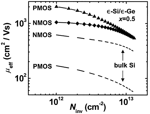
Figure 2: Heterostructures similar to the one shown in Figure 1 can support very high and nearly symmetric mobilities for both holes and electrons.
Reprinted with permission from "Strained Si, SiGe, and Ge channels for high-mobility metal-oxide semiconductor field-effect transistors" (J. Appl. Phys. 97[1]: art. no. 011101, 1 January 2005). Copyright 2010, American Institute of Physics. View article.
Figure 3:
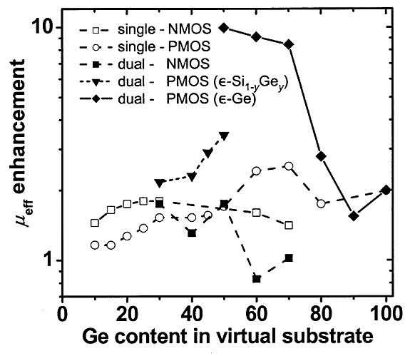
Figure 3: Map of all available mobility enhancements in single- and dual-channel strained SiGe heterostructures. At the midpoint, hole mobility enhancements of 10x and electron mobility enhancements of 1.8x are possible.
Reprinted with permission from "Strained Si, SiGe, and Ge channels for high-mobility metal-oxide semiconductor field-effect transistors" (J. Appl. Phys. 97[1]: art. no. 011101, 1 January 2005). Copyright 2010, American Institute of Physics. View article.