Harald Giessen & Na Liu
talk with ScienceWatch.com and answer a few
questions about this month's New Hot Paper in the field of
Materials Science. The authors have also sent along
images of their work.
Following the initial realization of optical metamaterials (Linden S,
et al., "Magnetic Response of Metamaterials at 100 Terahertz,"
Science 306: 1351-53, 2004) experimental and theoretical work grew
rapidly in this field. Metamaterials are structures which are much smaller
than an optical wavelength and often consist of metallic, plasmonic
nanostructures. They might have the potential for perfect lensing and
optical cloaking. However, most realizations of optical metamaterials were
just surfaces.
In order to obtain real three-dimensional materials, stacking techniques
were required. We give the first account of a stacking technique to obtain
3D metamaterials which is, in principle, not limited to a certain number of
layers. This work inspired a lot of follow-up papers which deal with the
optical properties of multi-dimensional, stacked metamaterials. Coupling is
very important in such structures, and its role needs to be clarified.
Does it describe a new discovery, methodology, or
synthesis of knowledge?
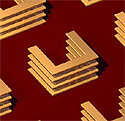
Concept drawing of stacked split-ring resonators
made from gold and stacked on a glass substrate
with polymer spacer layers.
View/download four
accompanying slides and
descriptions.
PDF
We have described how to manufacture 3D metamaterials with a planar
stacking technology which is industry compatible. In principle, a
semiconductor electronics lab could use our technology to produce up to
20-layer, 300 mm diameter, sub-100 nm structure size metamaterials.
Following our paper, other authors have come up with alternative methods
for 3D metamaterial fabrication (such as direct laser writing). Compared to
our planar stacking technique, there are advantages and disadvantages to
these other methods.
Would you summarize the significance of your paper
in layman's terms?
We describe a manufacturing method for 3D metamaterials. The method works
layer-by-layer, just like "building" a hamburger slice by slice until it is
really big and three-dimensional. The key to our method is to get the
layers planar after every step and to align the individual layers to each
other. You know this problem from a hamburger: if the layers are not
aligned, for example, the cheese might come out at the side.
How did you become involved in this research, and
were there any problems along the way?
We have been working on nanoplasmonics since the late 1990s, mostly in the
field of metallic photonic crystals, which have sizes on the order of half
the optical wavelength. Going to even smaller structures was the logical
consequence. Stacking is not trivial with electron-beam lithography
systems. We had to develop the planarization and alignment technology.
Where do you see your research leading in the
future?
With our nanotechnology, we are free to fabricate any layered nanophotonic
structure. This adds a whole number of degrees of freedom for the design of
such structures. For instance, it is possible now to not only use electric
dipoles that couple to each other, but also higher-order multipoles such as
quadrupoles or even magnetic resonances. This "optical magnetism" opens a
whole new door to building artificial functional nanostructures with
completely new properties that cannot be found in nature, for example, a
negative refractive index.
Do you foresee any social or political implications
for your research?
Actually, there are already theoretical concepts that describe optical
cloaks. This would mean that Harry Potter's vision of covering up might
come true one day. This would certainly have a lot of applications, and
only your own imagination would limit the possibilities of such a device.
Prof. Dr. Harald Giessen
4th Physics Institute
University of Stuttgart
Stuttgart, Germany
Na Liu, M. Sc.
4th Physics Institute
University of Stuttgart
Stuttgart, Germany Web