Colombo Bolognesi Talks about a High-Electron-Mobility Transistor
New Hot Paper Commentary, January 2012


|
Article: 205-GHz (Al,In)N/GaN HEMTs
Authors: Sun, HF;Alt, AR;Benedickter, H;Feltin, E;Carlin,
JF;Gonschorek, M;Grandjean, NR;Bolognesi,
CR |
Colombo Bolognesi talks with ScienceWatch.com and answers a few questions about this month's New Hot Paper in the field of Engineering.
![]() Why do you think your paper is highly
cited?
Why do you think your paper is highly
cited?
Our paper reported the very first gallium nitride (GaN)-based transistors to show cutoff frequencies exceeding 200 GHz. This breakthrough was accomplished using a new material combination involving aluminum-indium-nitride (AlInN), a compound semiconductor material largely pioneered in Prof. Grandjean's group at EPFL in Lausanne, our co-authors on the paper.
Up to the work described in the paper, this newer AlInN/GaN material combination always led to slower transistors than those fabricated in the conventional and more mature AlGaN/GaN system. This also certainly helped attract attention to the work.
Finally, workers in our field are very much focused on breaking barriers and setting new performance benchmarks: such results strike the imagination of contributors, and papers breaking the 200, 300, and 400 GHz milestones tend to generate much resonance in the community.
![]() Does it describe a new discovery, methodology, or
synthesis of knowledge?
Does it describe a new discovery, methodology, or
synthesis of knowledge?
As stated above, it showed that this new material combination had a lot more potential for high-speed performance than one could believe based on the previously existing literature.
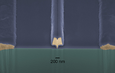
Nanometer-sized AlInN/GaN high electron mobility
transistor fabricated at the ETH-Zürich Millimeter-Wave Electronics Group.
The colorized scanning electron micrograph shows the T-shaped gate
electrode used to control the transistor current flowing between the
contacts on each side of it. The gate footprint determines the
transistor’s ultimate maximum frequency of operation, and is about
30 nm. The entire device is embedded in a thin passivation
dielectric.
Image courtesy of Stefano Tirelli.
![]() Would you summarize the significance of your paper
in layman's terms?
Would you summarize the significance of your paper
in layman's terms?
I would say that we showed that this new AlInN/GaN material combination can be used to fabricate the world's fastest GaN transistors. This is not only important because engineers want to make devices continually smaller and faster, but also because the AlInN material system offers the promise of higher component reliability when compared to the more mature AlGaN/GaN system. It sure is nice to be able to report record performances, but in applications devices must work reliably with a long lifetime before failure.
![]() How did you become involved in this research, and
how would you describe the particular challenges, setbacks, and
successes that you've encountered along the way?
How did you become involved in this research, and
how would you describe the particular challenges, setbacks, and
successes that you've encountered along the way?
When I first became a Professor, I decided to stay away from the field of nitride semiconductors: I thought it too late to join that bandwagon. Then, an industrial partner from the telecom field offered funding to work on GaN transistors. Professors always need more resources, and I thus accepted. A few years later, the company pulled its funding and started collapsing. Their organization almost entirely vanished, leaving me with some Ph.D. students midway in their degree, and with a keen interest in the topic. I just could not stop, and when I relocated to ETH, I brought the work along.
![]() Where do you see your research leading in the
future?
Where do you see your research leading in the
future?
The philosophy behind my group's activities has always been to develop the highest possible performance devices while trying to keep the fabrication process realistically "manufacturable" —as opposed to demonstrating record performances purely for the sake of publication and reputation. We want to work with companies, whenever possible, to see the concepts we develop in the lab find applications in the real world. Records do bring citations, but when a process can be transferred to industry, one finally has proof that the concept is indeed sound.
![]() Do you foresee any social or political
implications for your research?
Do you foresee any social or political
implications for your research?
Yes, but indirectly, through its potential economic and environmental impacts. Nitride-based electronics have the potential to significantly reduce energy consumption, because they allow many functions currently implemented by conventional (silicon-based) electronics to be carried out with higher efficiencies using so-called widegap semiconductors such as GaN or SiC.
Potential applications span telecoms, where, for example, this type of
transistor can be used to greatly increase the efficiency of wireless base
stations (which now stands at less than 20%). As well, nitride devices can
be used in a wide variety of power electronics applications such as voltage
converters, power supplies, and electrical motor drives. Some published
estimates promise up to a 25% decrease of the world total energy
consumption, if nitride technology were widely adopted by year 2035. Even
if this turns out to be only partially correct, it indeed remains an
exciting and worthy prospect.![]()
Colombo R. Bolognesi
Chair, Millimeter-Wave Electronics Group
ETH-Zürich / Swiss Federal Institute of Technology
Zürich, Switzerland
Web
KEYWORDS: ALINN/GAN, HIGH-ELECTRON-MOBILITY TRANSISTOR (HEMT), MILLIMETER-WAVE TRANSISTORS.